There’s a delicious technical symmetry to digital photography. The sensors that we use to take pictures are incredibly complex and intricate creations. And those sensors for photography are made my employing – wait for it – photography.
Did any of you say, “huh?”
I can explain. Those who know all this stuff can skip ahead. The sensor in your camera is a type of silicon-based integrated circuit. It consists of photodiodes to convert the light to electrical charge, transistors to buffer the voltage on the capacitor where that charge is stored, switches to allow the output of those transistors to be connected to analog-to-digital converters (which are themselves made of transistors and othe electrical components. Millions and millions (think Carl Sagan’s voice here) of devices are on that sensor.
How’d they get there?
Basically, they are printed on to a wafer of silicon. That statement is only true if you allow me a lot of latitude in the definition of “printing”, but it is a useful way to think about semiconductor fabrication. In a bit more detail, what happens is that the wafer of silicon has masks applied to it sequentially, and it is exposed to processing after each mask is applied that changes the nature of the material, or adds or subtracts material. Thus the integrated circuit is built up over many iterations.
So how to those masks get on the wafers? That’s where the photography comes in. The wafer is coated with a special photographic emulsion called a photoresist. Then the places where you want the mask to be are exposed to light. This used to be done in something like a contact printer, but now it’s done with something like an enlarger, only one that works backwards: the projected image is smaller than the “negative”, not larger. In the old days, with feature sizes of a couple of micrometers, the photoresists were of the negative type: the resist remained in the lighted areas when the wafer was “developed”. Now, with the details on the chip much smaller than that, photoresists are positive: the resist remains in the dark regions upon “development”.
I talked about “light” in the previous paragraph. It used to be that they used actual light that you could see. But as the features on the chips got smaller, they had to go to ultraviolet light, then very far ultraviolet. In the next generation of chips or the one thereafter, they will have to use wavelengths about 1/40th of that of blue light. Those are absorbed by air, and lenses are opaque to them. That makes for some interesting technical challenges and some very expensive equipment.
For a look at where semiconductor lithography (which is what the folks in the biz call the kind of photography I’m describing here), take a look at this.
Now, what’s that got to do with cost? As feature sizes have been decreasing over the years, the cost of the facilities necessary to make the chips (known as “fabs”) has skyrocketed. That hasn’t kept the semiconductor makers from chasing smaller and smaller features. A big reason is speed. The smaller you can make the circuitry on a chip, the faster it gets. Similarly, as the transistors get smaller, the power goes down. Another is cost: die area costs money, and the smaller you can make the circuitry, the less area you need. To see how this has played out over the last thirty or forty years, I looked at the size of the chip and the size of the features over that period for an Intel x86 processor. Where I could, I took the first generation of each new major design, ignoring “shrinks” that occurred after that. To get a length to length comparison, I calculated the length of each chip assuming that they were all square.
Here’s the table:

Then, I looked at a graph of feature size vs time:

Can’t see much in the later years, can you? How about a log scale:
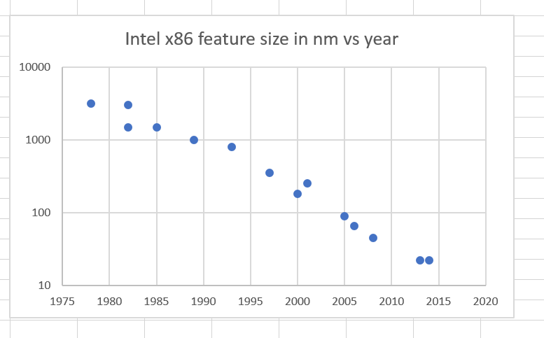
It’s pretty amazing how feature size is close to a straight line on log paper, except for maybe a flattening lately. That’s pretty much what Moore’s Law says has to happen if the chips don’t get bigger over time.
Let’s see if they do, calculating die size as if the chips were square from the chip area:
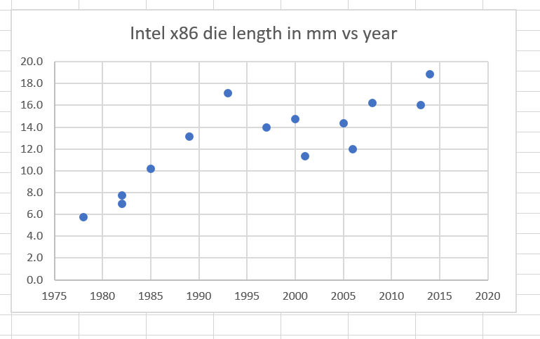
The chips have been growing with time, but very slowly compared to the way the features have been shrinking.
When you put the somewhat bigger chips together with the much smaller features, you end up with the number of transistors per chip being an even straighter line on log paper:
![]()
That’s what Moore’s Law was all about.
If the chip size had stayed the same as the 8086 chip size, and the number of transistors varied in proportion with one over the square of the feature size, the number of transistors per cip would have looked like this:
![]()
You can see that the chip areas have had to increase to keep Moore’s Law working.
There’s one imponderable here: how feature size is measured has not remained constant over the years. However, the changes in the definition have a small effect compared to the huge changes in lithography over the years.
Here’s the take-away: over the last 30 or 40 years, IC feature sizes have dropped in such a way as to allow exponential growth in transistors over that time, with some falloff towards the present which has been compensated by a modest growth in chip size. The reduction in feature size has come at a huge cost in the capital necessary to construc
You can see this dynamic playing out with sensors, although the data is not as readily accessible. Sensor size started small, increased a bit, and, for the largest consumer sensors peaked years ago at about 40x54mm. We have seen more and more full frame (24x36mm) sensors, at increasingly affordable prices in recent years. On the other hand, the bulk of sensors are now very small; they are made for cellphone cameras. In many cases, the tiny chips in those cameras have pixel counts equal to those of full frame sensors of a decade ago, and in at least one case, there’s a cellphone camera with a pixel count equal to many of today’s highest-resolution FF cameras.
In microprocessors chip size is a byproduct of the rest of the design, not a determiner of function in and of itself. That’s not true of sensors, where the size of the chip is related to the characteristics of the image captured. Large sensors can do things that small ones cannot, and large size is in some applications a good thing. So sensor economics are different from microprocessor economics.
So the question before the house is: given a sensor size — say full frame for the purposes of this discussion — what are the costs associated with increasing the pixel count? We’ve removed a degree of freedom normally available to an IC designer here: the ability to offset the cost of smaller geometry by making the chip smaller. Let’s constrain this discussion a bit by saying that we’re interested in the costs to reduce the pixel pitch from, say, 4.5 micrometers (um) to half that, or 2.25 um. The looser pitch would give us a 42MP sensor, and the finer one a 164 MP one. Those dimensions are large compared to modern feature sizes. However, many things are associated with a sensor pixel: a source follower (transistor and load), some switching, and, in the case of sensors with dual conversion gain, a capacitor. If the sensor is illuminated from the front side, all that circuitry gets in the way of the light falling on the sensor, and should therefore be small in size. So, although it’s not 100% essential, the tendency is to want to make the circuitry smaller if the pitch drops.
There’s another thing that makes a sensor designer want to make the features smaller if the pixel count goes up: without faster switching and analog-to-digital conversion, it takes four times as long to read the data off a chip that has four times the number of pixels. And we’d like faster readout speeds than what we’ve got now to increase video fps and make all-electronic shutter more useful. Speaking of all-electronic shutter, it would be a lot better if we had something called global shutter, which would allow the exposure to be started and stopped at the same time all across the sensor; that’s going to take more circuitry.
It’s not simple, but there are a lot of things driving sensor designers to make each pixel more complicated, and, even with modest feature shrinks, that competes with more pixels.
I haven’t mentioned yield. One, because I don’t know much about what the actual industry experience is (it’s a closely guarded secret at most fabs). But there’s another reason. Sensors are different from microprocessors in that they don’t have to work perfectly. Stuck and dead pixels can be detected and mapped out; this is routine for camera manufacturers. Possibly, although I think this would be pushing it, an entire dead column could be interpolated over. Even so, with no way to make a full frame sensor smaller, decreasing the feature size to cram in more pixels at some point will affect yield.
Put it all together, and it’s pretty mushy. but I don’t expect a quantum leap in pixel density any time soon, although I think we’ll see continuing improvements without material increases in price. And I don’t expect sensors to get much bigger.
If you are interested in optical lithography, I would recommend these two resources.
First, my late advisor worked at Perkin Elmer when photolith got off the ground. He wrote this piece some years ago: http://www.ora-blogs.com/kevin/2012/07/moments-in-optical-lithography-it-appears-i-was-there.html
Towards the end of this talk, the primary designer of most of the commercial litho lenses used by Zeiss (and thus, ASML) gives some insight into next-gen EUV systems.
http://www.slideshare.net/operacrazy/highlights-of-my-48-years-in-optical-design
You may be able to find better dirt in his other talks. He has gone into more detail in more recent times.
Hi Jim,
I don’t agree with this:
“There’s another thing that makes a sensor designer want to make the features smaller if the pixel count goes up: without faster switching and analog-to-digital conversion, it takes four times as long to read the data off a chip that has four times the number of pixels. And we’d like faster readout speeds than what we’ve got now to increase video fps and make all-electronic shutter more useful.”
Modern CMOS sensors seem to have column wise converters so with 4 times the pixels you would have 2 times the number of converters.
Regarding the mapping out of bad pixels/columns, Michael Reichmann visited Phase One in the old CCD times, perhaps 2005. There is a video at LuLa as far as I remember they talked about mapping out defective columns and also indicated that they had a pretty high rejection rate, the figure I recall was around 7%.
https://luminous-landscape.com/videos/luminous-landscape-video-journal-issue-14/interview-jesper-sandager/
(On average two bad columns and 300-400 bad pixels?, around 16 minutes into the video).
Erik, you’re right about the ADC speeds. For column ADCs, they would only have to run twice as fast. However, the total throughput for the sensor would have to quadruple. With column ADCs, as you say, you’d have twice as many, which you’d want to fit on the sensor without making it bigger, so a finer-geometry process would be welcome.
Thanks for the information about mapping out bad columns. I don’t see how it would be possible to do that without introducing artifacts that you could see with test targets, if maybe not with real-life images. When I use the Betterlight back and get a spot of dust on the sensor, that affects an entire row, and I sometimes find those artifacts difficult to remove without leaving a trace.
Jim
Hi Jim,
The way I see it, an increase in resolution is a way to avoid aliasing artefacts in the final image. But, it is very clear that increasing resolution is producing a lot of data, thus wasting storage space.
An approach I would consider is to have an option in firmware to downsample the image, using a simple algorithm. Just as an example, it may be that bilinear interpolations on a 64 MP image may yield better results than bicubic on a 16 MP image. So the user could make a choice between a large high quality file or a smaller but not so optimal quality file.
Best regards
Erik